
key steps involved in electronic circuit board assembly
Electronic circuit board assembly is a complex yet essential process in the manufacturing of electronic devices, encompassing a series of meticulous steps that culminate in the creation of functional and reliable circuit boards. From component placement to soldering, from inspection to testing, each step plays a critical role in ensuring the quality and performance of the final product. Understanding the key steps involved in electronic circuit board assembly provides insight into the intricacies of modern electronics manufacturing.
The journey begins with the preparation of the circuit board itself. This involves selecting the appropriate substrate material, typically fiberglass-reinforced epoxy laminate, and coating it with a thin layer of copper on both sides. The copper layer serves as the foundation for the conductive traces that will carry electrical signals throughout the circuit board. Once the substrate is prepared, the next step is to apply a layer of solder mask or solder resist, also known as coverlay, which helps protect the circuitry and define the solderable areas on the board.
With the substrate prepared, the next step in electronic circuit board assembly is the placement of electronic components. This process involves mounting various surface-mount and through-hole components onto the circuit board according to the design specifications. Automated pick-and-place machines are often used to precisely position components onto the solder paste applied to the board’s surface. The placement of components must be accurate and consistent to ensure proper electrical connections and optimal performance of the circuitry.
What are the key steps involved in electronic circuit board assembly?
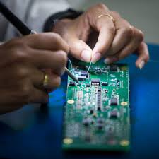
Once all components are placed on the circuit board, the next critical step is soldering. Soldering establishes electrical connections between the components and the conductive traces on the circuit board, ensuring the flow of electrical signals. There are several soldering techniques used in electronic circuit board assembly, including reflow soldering, wave soldering, and selective soldering, each suited to different types of components and assembly requirements. During soldering, the solder paste applied to the board’s surface is melted, forming solid solder joints that bond the components to the circuit board.
Following soldering, the assembled circuit board undergoes thorough inspection to detect any defects or anomalies that may affect its functionality or reliability. Automated optical inspection (AOI) systems and X-ray inspection techniques are commonly used to scrutinize solder joints, component placements, and overall assembly quality with precision and accuracy. Any defects identified during inspection are rectified through rework or repair processes to ensure the integrity of the assembly.
Once inspection and any necessary rework are completed, the final step in electronic circuit board assembly is testing. Functional testing verifies the functionality and performance of the assembled circuit board, ensuring that it meets the specified requirements and operates as intended. Various testing methods, including automated test equipment (ATE) and in-circuit testing (ICT), are employed to evaluate the electrical characteristics, functionality, and reliability of the circuit board under simulated operating conditions.
In conclusion, electronic circuit board assembly involves a series of key steps that are essential for the creation of functional and reliable circuit boards. From substrate preparation to component placement, from soldering to inspection and testing, each step requires meticulous attention to detail and adherence to strict quality standards. By carefully navigating through these steps, manufacturers can produce electronic devices that meet the demands of consumers for performance, reliability, and innovation in an increasingly interconnected world.