
PCB fabrication assembly work
PCB fabrication assembly is a complex and multi-step process that combines various technologies and techniques to create the backbone of most modern electronic devices. Printed Circuit Boards (PCBs) are the foundation that connects and supports electronic components, allowing them to communicate with each other in an efficient and organized manner. Understanding how PCB fabrication assembly works can provide valuable insights into the world of electronics manufacturing.
The process of PCB fabrication assembly begins with the design phase, which is the first and most crucial step. Engineers use specialized software tools to create a detailed schematic and layout of the PCB. During this stage, the placement of components, the routing of electrical signals, and the overall structure of the board are planned meticulously. The design is then translated into a physical form, ready to be fabricated. The design is critical because even minor errors at this stage can lead to functional issues or inefficiencies in the final product.
Once the design is complete, the fabrication process begins. PCB fabrication involves the creation of the physical board, which starts with a substrate, often made from materials like fiberglass or plastic. The base layer is coated with a thin layer of copper, which serves as the conductive material. Using a process known as photolithography, the copper layer is etched away to form the traces that connect the different components on the board. This step is done with high precision, as even the smallest misalignment can affect the functionality of the PCB.
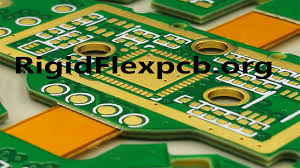
How does PCB fabrication assembly work?
After the copper traces are created, the next step in the PCB fabrication assembly is drilling holes for components such as resistors, capacitors, and integrated circuits. These holes are carefully drilled using computer-controlled machines to ensure accuracy. The drilling process is followed by plating, where the holes are coated with copper to allow electrical connections between the components and the board’s copper traces. In some cases, multiple layers of copper are stacked to create more complex PCBs with greater functionality.
Once the PCB is fabricated, the assembly process begins. This involves placing electronic components onto the board, which can be done using either surface-mount technology (SMT) or through-hole technology (THT). In SMT, components are mounted directly onto the surface of the board, while in THT, components are inserted into holes and then soldered in place. Automated machines play a significant role in this stage, placing the components with high precision and speed. The components are then soldered using reflow soldering or wave soldering, depending on the technology used.
After the components are attached to the PCB, the next step in the PCB fabrication assembly process is testing. The assembled board is thoroughly checked for defects and functional errors. Electrical testing ensures that all traces are correctly connected and that the board is free from short circuits or open circuits. In some cases, functional testing may also be conducted, simulating the real-world conditions the PCB will face in the final device. If any issues are found, the PCB is either reworked or scrapped, depending on the severity of the problem.
Finally, after the PCB has passed all quality checks, it is ready for integration into the final product. Whether the PCB is used in a smartphone, a medical device, or a home appliance, the quality of the PCB fabrication assembly directly impacts the performance and reliability of the end product.
In conclusion, PCB fabrication assembly is a detailed and precise process that involves several stages, from design and fabrication to component assembly and testing. Each step in the process is critical to ensuring that the final PCB is functional, reliable, and meets the required specifications. Understanding how PCB fabrication assembly works is essential for anyone involved in electronics design and manufacturing, as it is the key to producing high-quality electronic devices.


