maximum aspect ratio achievable for blind vias
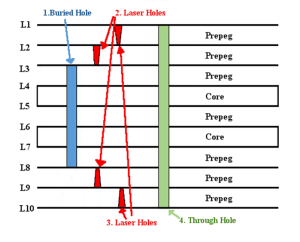
Generally speaking, vias are holes that are drilled mechanically on the PCB and then plated with copper to create an electrical connection. These connections are necessary to ensure that components are properly connected on the circuit board and that signals are transmitted from one layer to another. Vias are often seen in a variety of sizes and types, but they all serve the same purpose. There are three main types of vias in a PCB: through, blind, and buried.
The blind via is a type of hole that connects one outer layer with several inner layers and does not show on the PCB’s surface. Unlike through vias, blind ones do not connect layers on opposite sides of the board and are therefore a good choice for circuit boards with many layers. Adding them to a design can help boost signal routing and increase overall performance.
There are some limitations on the size and aspect ratio of blind via. The ratio of the hole’s height to diameter must not exceed 0.8, and they cannot start or end in the middle of the layer. In addition, they must be located far enough away from the edges of the layer to avoid damage during the manufacturing process.
What is the maximum aspect ratio achievable for blind vias?
A PCB with a high aspect ratio can be more complex than its counterpart. This complexity can lead to spacing issues that require meticulous planning. Attempting to add a blind via without this plan will create space problems that can be costly and difficult to resolve.
Despite these limitations, blind vias are a cost-effective option for circuit boards with a lot of layers. Compared to through-hole vias, blind ones offer higher transmission quality and can handle more signals in a given bandwidth.
The blind via is also ideal for making durable electronic products. Its lamination ensures that it will be able to withstand extreme conditions and continue to function efficiently for a long time. In addition, it allows heat to dissipate through the structure without damaging its internal components.
The manufacturing process for a PCB with blind vias is similar to that of a conventional multilayer board. First, a thin piece of laminate is cut to form two sided boards. Then, a detailed-above-process is used to drill and etch the blank, after which it is plated with copper. Finally, it is laminated with all other layers to produce a uniform multilayer PCB.
Using blind and buried vias can increase the density of a multilayer circuit board. This will allow for more functionality in a smaller area of the board, and will result in more efficient and reliable electronics. However, it is important to understand how these features work and their limits before using them in a production circuit board. This way, you can make sure that the final product will meet all of your requirements and provide the highest level of performance possible.